Coppersmith
Prototype your products with your own PCB designs.
In part 1 of this series on PCB design, I covered schematic capture in KiCad. The schematic embodies the logical part of the design, which components are used, and how they are interconnected. To complete the information required for PCB layout, the component symbols are annotated with data that describes the physical layout of the component pins, otherwise known as a footprint.
Other symbols represent mechanical features required by the design, such as mounting holes and any markings on the silkscreen layer. These elements can be added directly to the PCB layout without having a reference in the schematic. You can also mark such things as logos, copyright warnings, and revision numbers to be excluded from the bill of materials (BOM) in the symbol’s properties.
In this second, concluding part of the series, I walk you through the process of laying out and tracking your PCB and producing manufacture-ready files.
Layout Process
The output of the layout tool is a set of Gerber files that describe the track pattern that must be etched onto each copper layer and Excellon files that describe the hole pattern that needs to be drilled for your PCB. Additional Gerber files describe solder masks, paste masks, silkscreen printing instructions, and the like. This data can be sent directly to manufacturers, who produce a PCB to the exact design in the layout.
The ordering process generally involves filling in an online form that specifies overall dimensions, PCB material and thickness, solder mask color, and silkscreen layer color. You will be asked to upload the pcbnew.zip file containing the plot output of the KiCad PcbNew layout tool. If you stick to a board size of less than 100x100mm with two copper layers, the PCB manufacturers will produce five or so PCBs for around $5 (EUR5/£5) and ship within three days. Often, the shipping is more expensive than the PCB production, so I tend to batch up my designs and order them together when possible.
Most companies understand the default file names that KiCad assigns to each layer, so you don’t need to rename them. Simply zip up the contents of the plot output directory and give it a meaningful name. Appending a revision number to this file (e.g., kitchen_timer_REVA.zip) ensures that if you ever want an updated version manufactured, there’s no possibility of confusion. I’ve found that manufacturers check the data you send them carefully and will reject the design if it does not meet their design rules or if they spot things that might compromise your design. Be prepared to take their advice and make small changes; it will save you money and ensure your PCB has the greatest chance of working.
KiCad’s PCB Editor provides a graphical view of your layout with different layers drawn in different colors. You can switch the visibility of layers so that you can concentrate on the task at hand. For a two-layer board, the minimum layers you’ll need to work on are front and back copper, front and back silkscreen, and the board outline, known in PcbNew as “edge cuts.”
If your board has large apertures of irregular size, they are drawn on the edge cuts layer, too. Other layers essential to manufacture are solder mask layers, which prevent bridging of solder resist between component pads and tracks, and paste layers, which are used to generate an optional stencil, available at extra cost for use as a mask to put solder paste onto component pads for infrared soldering.
Importing to PCB Editor
Start the schematic editor from KiCad’s project interface, and once you are happy with the schematic, select Tools | Update PCB from Schematic. If the file does not exist, KiCad asks whether you want to create a PCB. The dialog box (Figure 1) shows the update process and PCB Editor opens in the background. If you see errors, you can cancel this dialog and go back to fix them, repeating this process until all the errors are cleared.
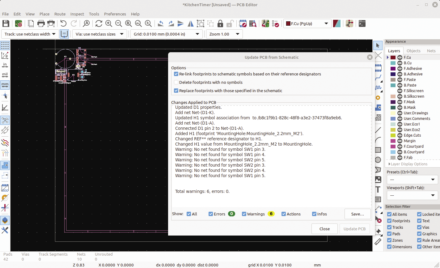
Although you can choose to proceed with errors (e.g., missing footprints), I don’t advise doing so until you are familiar with the process, because KiCad will simply omit parts with errors and you might end up with an incomplete design. When you are more familiar with the update process, it can be useful to proceed with errors because it allows you to get an early view on the eventual size of your PCB or to do other checks that require the PCB to be at least partially complete. Eventually, you will need to have an update that finishes with no errors to ensure your design is completely transferred.
The components are arranged at the top left of the editor; select the Update PCB button and close the dialog. You have successfully transferred your schematic data to PCB Editor. If you subsequently make changes to the schematic, you can repeat this process. Pay attention to the options in the dialog; you might need to change the defaults.
Notice that the nets connecting pads are represented at this stage by thin white lines that go directly from pad to pad: This layout is known as the “ratsnest,” and part of the process of laying out a PCB involves replacing every segment of the ratsnest with a track on one or more of the copper layers in a manner that does not violate design rules.
Reusing an Existing Board Outline
If you have an existing design and want to reuse the board outline and other mechanical features, copy the PcbNew file into your new project directory and rename it to match the project’s schematic. When you open this file with PCB Editor, delete all the components, tracks, and anything else you don’t require. Now you can do the initial update from the schematic, and the file you’ve just modified will be opened and components and tracks from your new schematic added to it. If you want to retain features such as mounting holes, ensure you have matching components in the schematic and that their identification numbers (H1, H2, etc.) match.
PCB Editor User Interface
The usual top-level menu of PCB Editor gives you access to most of the tools you’ll need, in particular File | Board Setup, Place, Inspect | Design Rules Checker, and Preferences. The View | Units option allows you to switch between imperial and metric units. In the past, components tended to have pins on a 0.1-inch grid, but today’s parts come with all sorts of pin spacings, and dimensions are usually metric. As a European, I generally use a metric grid, but occasionally a part datasheet will have dimensions in imperial units; then, it is very useful to be able to measure in those units.
The toolbar has two important items: Print lets you use print-specific layers for desk-checking, and Plot plots the Gerber files for manufacture. Below the toolbar is a Grid drop-down. KiCad by default draws with snap-to-grid, and you’ll want to change the grid depending on what you are doing (e.g., when you are drawing the board outline).
The Layers tab to the right allows you to select the active layer (i.e., the drawing layer). You can hide specific layers by clicking on the eye icon and change the layer color by double-clicking on the colored square on each layer. The Objects tab to the right of Layers is where you show or hide specific classes of objects, and the Nets tab allows you to show or hide nets by net class.
The bottom of the editor window shows the currently selected grid size and updates the cursor position in real time. The coordinates on the left are relative to the “drill place” origin, and those on the right are a relative position. Pressing the spacebar resets the relative origin, which is very useful for placing components relative to one another on a fixed point on the board.
To the left of the Layers tab is a vertical toolbar. The most useful of these tools are Toggle Ratsnet, Route Tracks, and Interactively Measure. The ratsnest – the untracked connections in the view you see after the initial update – slowly disappears as you route each track, but sometimes you want to hide these untracked connections so you can see the layout more clearly. An untracked board can appear very cluttered, and in general, the more layers and so on that you can suppress until you need them, the easier the layout will be. Interactively Measure is handy for measuring things such as pad spacing or the distance between traces.
Backups
KiCad keeps regular backups in the <Project-name>-backups folder below the main project directory. These backups are ZIP files annotated with the project name, time, and date, so if you get in a mess, you can unzip one of these and continue from that point.
Footprint Editor
As a further aside, if you really can’t find a footprint for a particular component, you can create your own with the footprint editor, which you start from the toolbar in PCB Editor or from the project interface. If you can, choose an existing similar footprint and use that as a guide. In any case, you need first to create your own library (I usually call this project footprints) and save it to the project directory. The editor itself has many of the same Place menu items as PCB Editor, with the addition of Add Pad.
You need to add a pad for each pin on your component as a surface-mount or through-hole pad, along with the pad shape, size, and, where applicable, hole size. Pay attention to the minimum annular ring design rule: The radius of the pad must be larger than the radius of the hole by a distance exceeding the minimum annular ring dimension. KiCad automatically adds text on the silkscreen and the fabrication layer: You can move those to a position of your choosing. To add the pads and pins you require at the correct spacing, use the measuring tool from the vertical toolbar and set the grid to the grid of the component pins, if possible. Save your new footprint to your new library. KiCad won’t let you modify footprints in its own libraries because they are read-only.
To use the footprint library you have created you need to add it to your project’s list of known libraries with Preferences | Manage Footprint Libraries and select Project Specific Libraries. Any footprint you have created should now be visible both from the schematic and PCB Editor.
Know Your Manufacturer
The first step in PCB layout is to tell KiCad the design constraints published by most manufacturers on their website. For instance, an extract from the PCBWay site (Figure 2) shows quite a lot of information, but the most important is minimum trace width and spacing, minimum drill size, and minimum annular width.
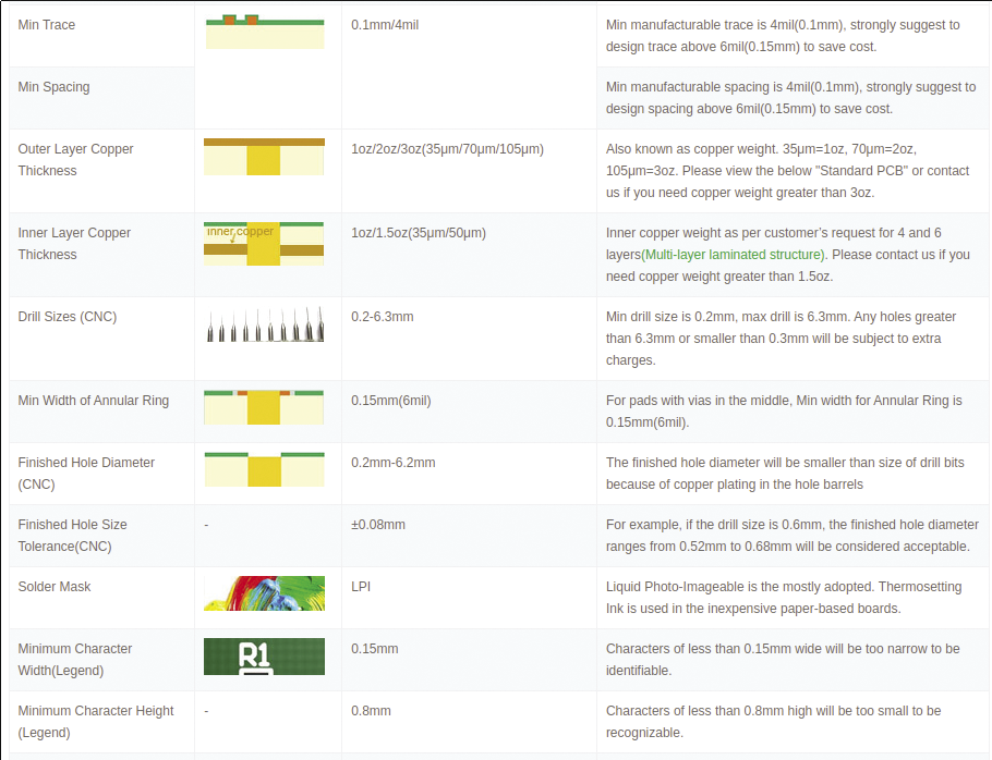
In PCB Editor select File | Board Setup and Design Rules | Constraints from the list on the left. The KiCad default values are within the capabilities of my manufacturer of choice and are fairly normal for today’s standards. If you go below these limits, your design may be rejected by the manufacturer or the price may go up steeply, so think carefully before making any changes.
Now select Text & Graphics | Defaults from the list. Again, you can check these numbers against the manufacturer’s capabilities. On dense PCBs, the default text size can make finding space for component identifiers and the like difficult, so I tend to reduce the text width and height of the silk layers to about half the default. The text is less readable to be sure, so this is a matter of taste and experience. You can always refer back to the design files when assembling and debugging. I usually print out an enlarged version of the silk layer to help. You can override any specific text item in its Properties (right-click), so you are not limited to the defaults.
Net Classes
In the schematic editor, you can annotate particular nets with net class directives. In the kitchen timer example used in this article, I added one directive: Power for the +3V and GND nets. Now if I select Net classes in the Board Setup dialog, I see two net classes: Default and Power. Any net that you have not annotated will fall into the default category, so you can set the track width and clearance for your “normal” tracks here, bearing in mind the overall constraints you have already set. The Power nets that were annotated can be given a wider track width. If you will be designing with high-voltage tracks, which require greater separation for safety reasons, you can also set the clearance to meet these requirements.
As a final step, select Board Stackup | Physical Stackup from the list. The layer count should be set to 2, unless you plan to design with inner tracking layers or power planes. Most manufacturers will produce boards with up to eight inner copper layers, but the price goes up exponentially with layer number. For simple designs, two layers is adequate, and you can flood fill either one or both outer layers with copper to give an almost complete ground plane (more about this later).
Take a look at the Board Stackup | Board Editor Layers item. You can deselect all the layers below Margin. Most of these layers are auto-generated, so don’t be overwhelmed. Generally, you have to edit manually only the copper layers, the silk layer, the board outline, and optionally the user drawings.
Board Outline and Dimensions
Before you can start placing parts and drawing tracks, you need a board outline. Select the Edge.Cuts layer from the Layers tab to the right and use the Place | Draw Rectangle, Place | Draw Line, and similar menu items to draw your outline.
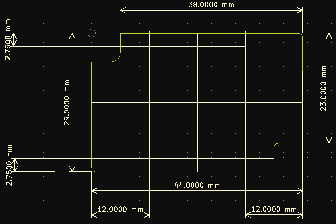
If your project does not have specific size or shape requirements you can simply draw a rectangle that looks big enough to place the components within and start to arrange them, adjusting the size as you go, once you have a feel for the layout and the amount of space for tracks between components. In the case of my example, I had already chosen a very small plastic enclosure made by Hammond manufacturing (part number 1551NBK). The enclosure drawing includes the maximum board outline that will fit, together with the location of two mounting holes, which you can use as the basis of your outline.
The board outline is drawn on the Edge.Cuts layer, so make sure you select that. Set the grid size to something in the region of 1mm initially. You might need to make this number smaller if the dimensions you are copying from don’t sit on 1mm boundaries. Set the grid origin to a point close to the top left of the drawing screen with Pace | Grid Origin, and put the drill origin at the same point with Place | Drill/Place File Origin. Use this point as the top-left corner of your board outline.
You can add dimensions by switching to the User.Drawings layer with Place | Add Orthogonal Dimension and similar items. The mouse wheel lets you zoom in and out – even in the middle of drawing a line, for example, so you can zoom in on your target. Your board outline should have no gaps: Various other KiCad tools will throw errors if the outline is incomplete, and your manufacturer might also reject your design or arbitrarily complete it for you.
If you want apertures in your PCB, simply add them to the Edge.Cuts layer within the board outline. You can annotate them with text on the dimensions or comment layer, but I have found that manufacturers correctly interpret any closed shape within the main board outline correctly, as long as it’s drawn on the Edge.Cuts layer. On the user drawing layer (Figure 3) you’ll notice I’ve added lines that intersect where the mounting holes should be placed, which will help align those holes when I come to place them. If you prefer, you can add these “construction” lines to another layer such as User.Comments, so you can hide them once placement is complete.
Laying Out Components
Now you can start to drag the components from their current position to within the board outline you’ve drawn. Turn off the front fab (F.Fab) and back fab (B.Fab) layers and set the grid to something small (e.g., 0.1mm), so you can place components precisely. You might also want to switch off the silkscreen layers until you’ve got a rough layout, but make sure the .Courtyard layers are visible; as you place components, ensure the courtyards do not overlap. To select a component and move it, just click and drag. Whilst in the drag mode, pressing r rotates the component by 90 degrees, which you can do repeatedly, and pressing f flips the component to the other side of the PCB.
In the example, the battery and connector are on the opposite side of the PCB from all the other components. Start with the components whose position is fixed, such as mounting holes, and drop them onto the construction lines on the User.Drawings layer. You can lock them in place by pressing l on a selected component. Place connectors next because they generally have some mechanical constraint in terms of location relative to the enclosure or other parts of your design.
If you have sensitive parts of the circuit (e.g., low-level analog parts), you’ll want to group those together. If you keep your schematic open, you’ll notice that selecting a component in the layout will highlight its symbol on the schematic, and vice versa, which can be useful in locating a particular component among the jumble of components from the initial update.
Keep the ratsnest visible: As you drag components around and locate them, try to minimize the complexity of the ratsnest to make routing the connections into tracks easier and more direct. Look at the .Courtyard layers and make sure the courtyards of adjacent components on the same side of the PCB do not overlap to ensure no mechanical interference between components when you come to assemble the PCB. KiCad will flag overlapping courtyards during the design rule check you’ll perform toward the end of the layout process.
When you have a tentative layout, you can turn on the silkscreen layers and place the identifiers. Selecting an identifier highlights the component to which it belongs, so you won’t inadvertently place an identifier with the wrong component. The component identifiers on these layers can be rotated and placed independent of their components, so you can orient them all in the same direction and place them as close as possible to the component. I try to position the identifier close to pin 1 of its associated component, where applicable, as an extra indication of the component’s orientation.
When drawing a schematic, separating some components to one corner of the drawing, or even onto a separate sheet, is often convenient. One case in point is decoupling capacitors. In digital circuits, good practice is to have at least one 100nF capacitor per integrated circuit: Microcontroller datasheets generally recommend several – at least one per power pin.
The point is that, although the decouplers may be hidden away in a corner of the schematic, you can’t simply lump them together in a similar way on the layout: They must be placed close to component power pins, with their ground connection directly grounded, preferably to a ground plane, to have a good chance of decoupling noise and preventing erratic system performance. Therefore, as you lay out your active components, be sure to leave space for decoupling capacitors at suitable locations close to the power pins of active components.
Adding 3D Models
Once you have a tentative layout, taking a look at the 3D view of the PCB is a good idea, because visualizing the complete assembled PCB from the layout tool alone can be difficult. The 3D Viewer, launched from View | 3D Viewer (Figure 4), generates a near-photo-quality 3D image that scrolls and pans and shows any unexpected interference between components. You can check the readability of the identifiers on the silkscreen layer.
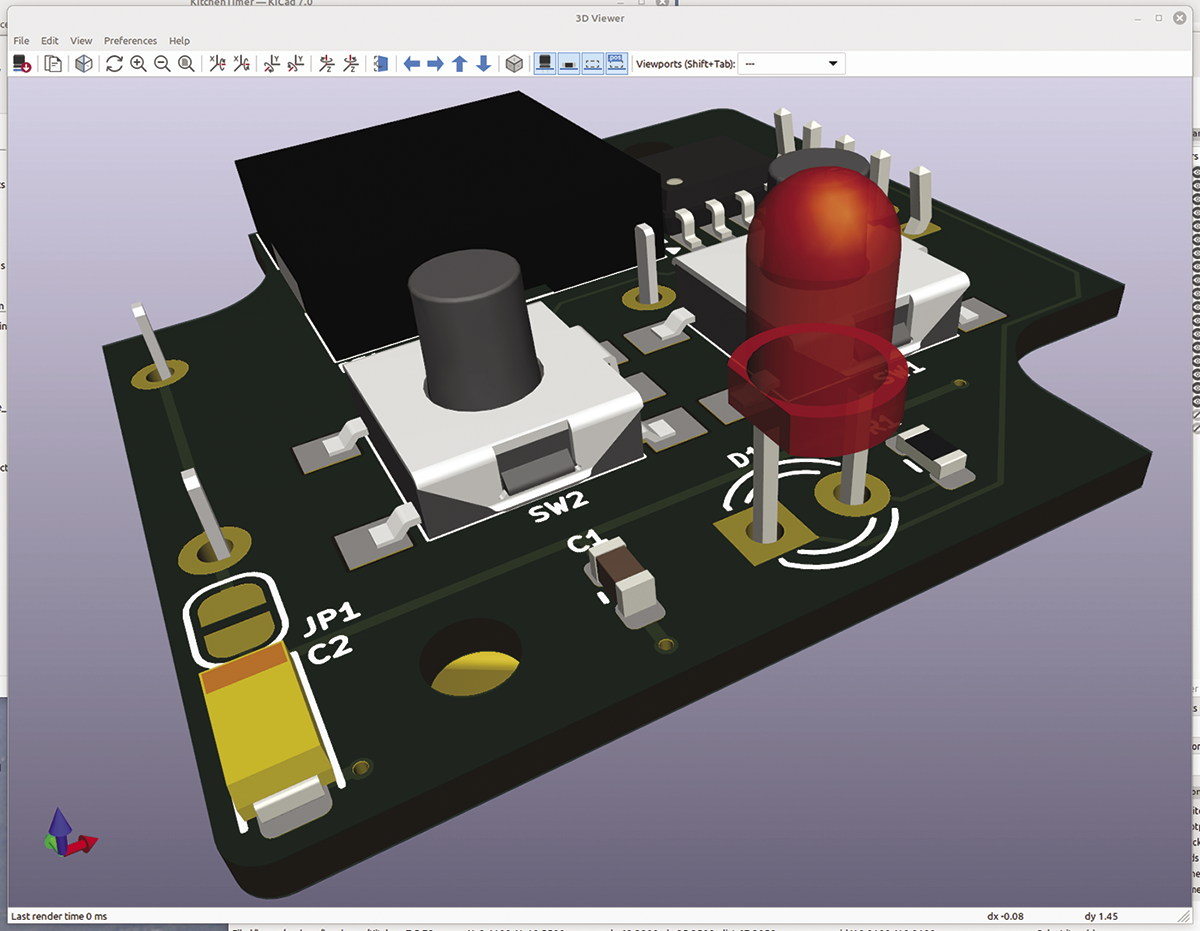
As you proceed with layout and subsequently tidy up the silkscreen layers and add any extra text, 3D Viewer shows an excellent overview of the end result. Some components might not have 3D models attached by default, especially if the component or footprint is not from the KiCad standard libraries. If you can find a 3D model from one of the many sites online, such as 3D ContentCentral, you can add it by clicking on any component footprint, selecting Properties, and clicking the 3DModels tab. The dialog allows you to scale, rotate, and move the model until it sits in the correct place on the footprint.
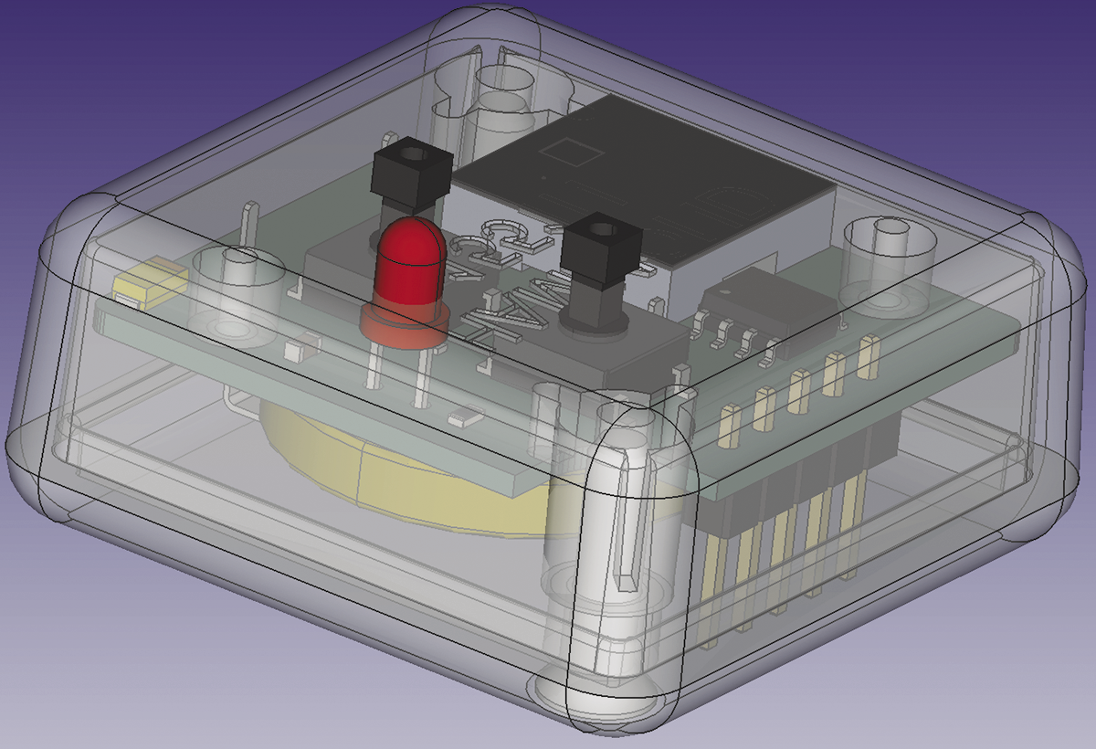
If you have an enclosure in mind with a STEP file, you can export a STEP file for the assembled PCB (File | Export | STEP) and build a model of the overall assembly in a mechanical CAD tool such as FreeCAD (Figure 5). At this point, it is a good idea to lock in place any components (e.g., connectors) that must not be moved because of mechanical constraints.
As you progress with the layout, you’ll undoubtedly want to make small adjustments to placement and orientation of small components to help with tracking, yet avoid moving other components. You can select multiple components to move as a block, and locking a component (pressing l) prevents it from being moved inadvertently. At the bottom right of the layout tool is the Selection Filter pane if you untick Locked items, they won’t be included in any multiple select, which is achieved by dragging the mouse across an area with the left button held down. Once you start tracking (i.e., replacing the ratsnest with tracks on the copper layers), the more pins a component has the more disruptive a move will be, so consider carefully the position of things like microcontrollers and connectors with a high pin count.
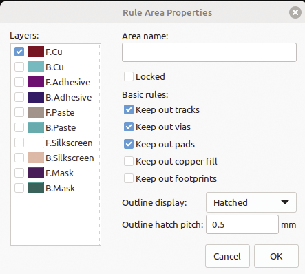
If your board requires physical separation between different parts of the circuit (e.g., between a mains power supply and the low-voltage digital area), you can use one of the User layers to draw filled shapes (e.g., draw a rectangle, select its Properties, tick Filled Shape) and use that as a reference when placing components and tracks. You can also place rule areas on any layer with Place | Rule Area and select rules such as Keep out footprints, Keep out tracks, or both, which prevents these items from being placed in the rule areas (Figure 6).
Laying Out Tracks
All of the preparation you’ve done up to now should make laying out tracks simple. Set the grid to the smallest possible (0.01mm, 0.0004in) so you can lay out tracks without constraint. The net classes defined earlier will mean power tracks will be wider and the spacing between may be larger if that’s what was specified. As a rule of thumb, try to keep one layer for tracks running up and down the board and one for tracks running from side to side. You will inevitably have to break this rule eventually, but if you route all your tracks at random from the start, you’ll end up with more vias (points where the tracks change sides) and a generally messy layout.
Start by routing the power tracks because these should be kept as short and direct as possible. If you plan to use a copper pour layer for your ground connections, you can ignore the ground net for now, or simply terminate it to a via at a point close to each grounded pad. Through holes that are grounded require no action because the copper pour will automatically connect to them.
The Route Tracks function is in the vertical toolbar to the right. Select one of the copper layers (most probably the top copper to start with because that’s where most component pads will be), click on a pad that has a ratsnest (the thin white lines connecting pads), and begin drawing a track by moving the mouse. You’ll notice that the track will only be drawn horizontally, vertically, or at 40 degrees. Make your way to the destination pad and click to draw your first track.
Don’t try to lay out the tracks perfectly at this stage: Concentrate on getting from source to destination, changing layers if necessary. Tracks can be pushed around and modified later but at the start it is enough to simply ensure that all tracks have valid routes. To change layers whilst in route mode, first add a via at the current location by pressing v. Next, change layers by pressing Page Down to go from top to bottom layer or Page Up to return to the top. You can then continue to route the track to its destination. You can also change layers as you did previously from the Layers tab at the right. I prefer the keyboard shortcuts to keep the mouse at the current track location. Once you have a few tracks routed, you can start to tidy them up.
Exit the route tracking mode by pressing Esc, select a track segment (defined as a length of track between two corners), and press d. You can drag the track around to where you want it; notice that you can push other tracks around with it, known as Shove mode, whilst maintaining the minimum spacing allowed by the design rules. Other modes are selected by right-clicking on the Route Tracks tool. Walk Around mode will not shove other tracks, and Highlight Collisions mode highlights other tracks if you try to route too close to them. Each mode has its use, but for the most part, stick with Shove mode.
Routing tracks is a bit of an art and takes time to learn effectively. Don’t be afraid to delete your tracks and try again. If you delete a segment, or several, you can go back into Route Tracks and re-route the section of ratsnest that reappears. Track segments have a Properties menu accessed with a right-click, and many tracking operations can be performed from there. In particular, you can change the track width (if you need to pass between two close pins, for example, to beef up a track carrying power, or to set the correct width for a controlled impedance track, such as a PCB antenna).
Copper Pours
A copper pour (sometimes known as a flood fill) covers the whole of a copper layer with copper, whilst avoiding all the tracks on that layer, leaving a gap between the fill and the tracks equal to the spacing you set in the board setup. Pours such as this are often used to provide a ground plane (i.e., a nearly continuous plate of copper on one or both layers). Copper pours help reduce electromagnetic interference (EMI) and are a convenient way to ensure all your components are connected to a solid ground.
Grounding and EMI are beyond the scope of this article, but suffice to say that good grounding is key to producing reliable operation, especially with high-speed devices or when high currents are involved. As I mentioned earlier, if you choose the lower copper layer for your ground plane, you can connect grounded pads on the upper layer by adding a via close to the pad and connecting it with a short track. Don’t be tempted to put a via coincident with a surface-mount pad: The manufacturer is unlikely to accept this layout. The via can be very close, however.
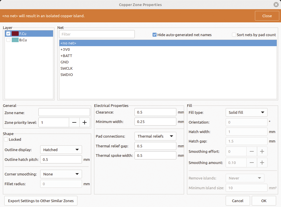
To add a copper pour, first set an appropriate grid (e.g., 1mm or 0.1in), select the target copper layer, and select Place | Add Filled Zone. Now select the required layer and select the GND net. Draw a closed shape that encompasses your required copper pour area. You can edit this shape by selecting it, adding or removing corners, and dragging corners to new positions. Now press b. As long as the area includes at least one pad, pin, or via connected to the GND net, the area will be filled with copper. If you want to remove the pour temporarily to see the layout more clearly, use Ctrl+B. If you move tracks around on a layer with a copper pour, the pour is not automatically updated, and you must press b, so it is often simpler to remove the pour temporarily with Ctrl+B.
Notice in the dialog in Figure 7 the settings for Clearance, which is the space the pour leaves between the pour and tracks. Other settings control thermal reliefs, which leave a gap around a ground pad in a ground plane, with spokes to ensure connection. Without these reliefs, it can be challenging to solder to these pins because the pour sucks away heat and prevents solder from flowing properly. Leave the settings at the default values unless you have a good reason to change them.
Silkscreen and Identifier Layer
Once you have components placed and all the nets tracked, you can tidy up the silkscreen layer. To begin, turn off the copper layers and any others you don’t need for now. If you have components on both sides, the bottom silkscreen will appear with text backward because you are effectively looking through the PCB. Choosing View | Flip Board View allows you too look at the board from the underside. In any event, you can now move component identifiers to their final location, rotating them as necessary. I like to have all my identifiers facing the same way, but that’s purely a matter of taste. All text items have properties, so you can change the size of the text should you so wish. You can add other text with Place | Add Text and even add lines and arcs to the silk layer. Text overlapping other text or any other feature on the silk layer will generate errors when you come to check the design rules.
Design Rules Check
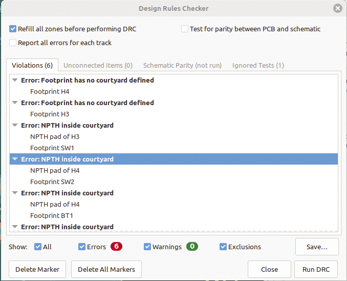
The most important step before you send your files to the manufacturer is to run the design rules check (Figure 8), which is accessed from Inspect | Design Rules Checker. To run the checks, click Run DRC. This tool is very picky. Some errors it reports will not cause manufacturing problems; you can choose to ignore whole classes of tests on the Ignore Tests tab. You can also exclude specific violations by right-clicking them in the list and selecting Exclude This Violation. Nonetheless, many of the errors, such as net spacing violations or incomplete tracks, must be corrected. Make sure you understand an error before choosing whether to correct or exclude it.
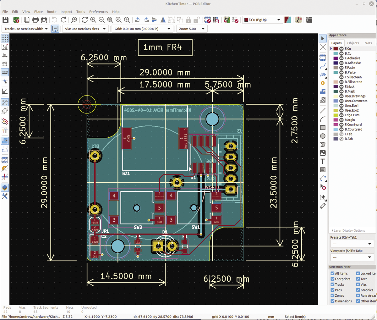
At this stage your PCB is complete (Figure 9). You have a board outline, tracks on the copper layers, and silkscreen layers with component identifiers. You’ve run the design rule check and satisfied yourself that the design is ready for manufacture.
Plotting Files for Production
When you have done all the checks you can, it’s time to plot the manufacturing files with Files | Plot. In this dialog (Figure 10), select the layers you want to plot in the Include Layers list. You should not need to change anything else without a specific request from your manufacturer. Add gerbers or any other directory name of your choosing in the Output directory field at top; press the Plot button and the Gerbers will be plotted and saved in that directory.
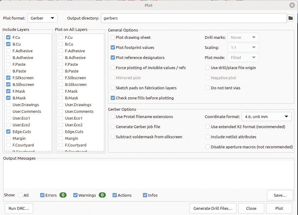
Before you close the dialog, click Generate Drill Files twice in two dialogs. Again, leave all the settings in this dialog as they are. These Excellon format drill files tell the manufacturer where to drill the holes and what size. The result is two files: one for plated through files and one for holes with no copper plating.
Optionally, you can select Generate Map File, which generates a human-readable PDF with a map of the holes and their sizes. It’s well worth checking the hole sizes against the component data sheet, especially if you’ve generated your own footprints or downloaded them from a random website. Connectors and transformers, in particular, have thick pins, and if the holes are too small you’ll have problems at assembly time.
Be aware that plated through holes will be slightly smaller than the size you specify because of the plating and solder tinning. The footprints in the KiCad library take account of this, so you can use these as a reference. It’s generally better to have slightly oversized holes than those that won’t accept a pin, so size the holes with a margin of around 0.1mm.
I recommend printing out the copper layers at 1:1 as a final check. If you have the parts to hand, you can physically place them on the printout to check that the footprint is correct. This simple step has saved me from embarrassment on more than one occasion. To print the copper layers, use Files | Print – or better still, use the Gerber View tool from KiCad’s project interface to open the manufacturing files you have plotted and print from there. It’s a good idea to measure on the printout something of known size with a ruler. If it’s in error, calculate the scale factor required and add that in the print dialog until your printouts become truly 1:1.
If you want to print solder paste to your PCB, as mentioned in the “Layout Process” section, you will need to add a stencil to your order. Simply make sure to include the Front Paste (F.Paste) Gerber file in your ZIP file. The stencil is a thin metal plate with apertures wherever you want to put solder paste. Place this stencil over your PCB, aligned with the pads, and wipe solder paste over the stencil. Let the paste to dry for a few minutes then remove the stencil. (An excellent online tutorial shows how to use stencils.)
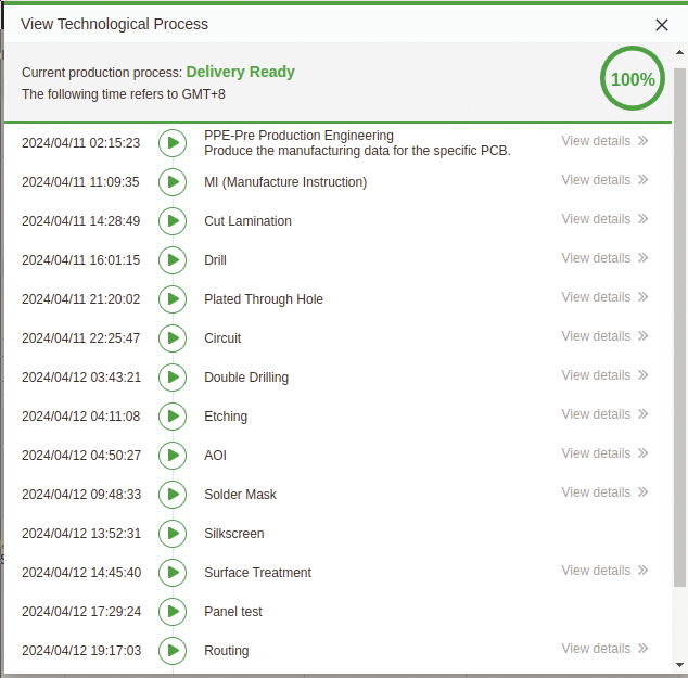
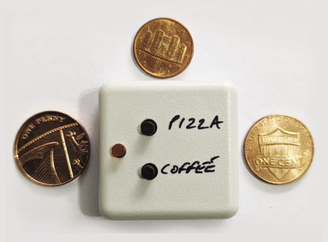
Once manufacturing gets underway, you can sit back and relax. The manufacturer works through all the required steps (Figure 11), and your PCB will be delivered ready for assembly. Figure 12 shows the example used in this article series assembled and ready for use.
Wrap Up
If this article has a theme, it is: Check your data! An incorrect wire here or there is fixable with cuts and straps, but an incorrect footprint or a plated hole that’s too small for its pin can stop your project dead in its tracks. The manufacturer will reject a design that violates its design rules, but they can’t know what components you are using and will make the PCB faithfully to the specifications of the Gerber and Excellon files you supply.
As mentioned previously, KiCad has its own Gerber file viewer, which is very useful for final checks. You can load several layers (e.g., the top and bottom copper) to ensure everything lines up or achieve a similar effect by turning layers on and off in PCB Editor. However, the Gerber files are the manufacturing data, so you are checking exactly what will be produced. The Gerber Viewer loads Excellon files, too, so you can check the position of mounting holes and the like.
Designing your own PCB, with the low cost of manufacture and rapid turnaround, makes much more sense for your money than other forms of prototyping. You get a professional looking product that will be much more robust in the long term, is easy to replicate reliably, allows for much more dense component layouts, and lets you use tiny surface-mount parts that would be nigh on impossible to use in any other way.
If you are not confident of being able to assemble parts of this type, many manufacturers also offer an assembly service and will even source the components for you. I’ve used this service in the past, where I’ve used a part that I can’t solder myself. If you plan to apply solder paste for infrared reflow assembly, remember to order a stencil.
Also worth noting it that many of the manufacturers who offer PCB services like this for small-run prototypes also offer exotic PCB materials, including flexible PCBs, and even 3D printing and CNC machining, as well, so you can have a one-stop-shop for your project.


