Designing PCBs
Take your electronic projects to the next level with your own PCB designs.
Many makers start in electronics by using pre-built modules: typically a module with a microcontroller (e.g., Arduino, Raspberry Pi, ESP32, or STM32 variant) and another board with some type of I/O (e.g., an accelerometer, camera, temperature sensor, or relay). They join these boards together with wire links, often without the need for soldering, to make a functional prototype. So far so good. The advantages of this approach are flexibility, speed, and low cost: They can keep making changes until they have the required functionality.
However, projects like this can be difficult to package in a compact manner and inevitably contain unneeded circuitry, and the wire links might not be durable over time. It can also be an expensive solution if more than one prototype is required. If you want your project to use a component not available on a module, run from batteries, have custom displays, or any variety of requirements, the need for a more flexible solution becomes yet more apparent.
You might move on to other prototyping systems, like soldering components onto a stripboard and wiring them up with soldered wire links. This approach worked well when I started out in the business 40 years ago, but today, many interesting components are just not available in through-hole form on the 2.5mm/0.1-inch pitch that was the standard back then.
When it comes time to send your design to production or start a design that cannot be achieved by hooking up standard modules, designing your own printed circuit board (PCB) is the way to go. The form factor is much more flexible when you design your own boards that can be shaped to fit into a commercially available housing, match up with provided mounting pillars, fit into a custom shape such as a model aircraft, or act as a plugin to an existing module such as a Raspberry Pi.
In recent years the software tools to design PCBs have become freely available, both in the commercial and open source worlds. Several companies now exist that will take your PCB design files and make a handful of PCBs for less that $5 (£5/EUR6) within a few days, so the cost of entry into this technique is very low. In this article and the next, I demonstrate what is required to have a PCB manufactured, from an initial idea to a completed PCB arriving at your door, ready for assembly.
What Is a PCB?
I am sure you have seen PCBs: They are in every piece of electronic gadgetry around your home, in your car, and in the office, from the simplest light switch through mobile phones to supercomputers. Your PC’s motherboard is a prime example. Simply put, PCBs carry the integrated circuits (chips) that make up modern electronics, together with other passive components such as resistors and capacitors, connected together to form a functional circuit. The term “printed” is a misnomer because PCBs are made by lithography, not printing, with only specialist circuitry made by printing metallized ink onto ceramic substrates.
The most common PCB substrate is FR4, a glass-reinforced epoxy laminate that is initially covered in a thin layer of copper (around 30µm thick) on both sides and then selectively etched to produce the pads and tracks that make up the mounting points and connections for components. Holes are drilled through the laminate before etching, and the walls of these holes are then plated with copper. If copper surrounds these holes on both sides, the two sides and the walls form a continuous copper surface, and once the etching is complete, tracks on either side of the PCB are connected electrically wherever they encounter such a hole. These connections are known as “plated through holes” or “vias.”
Components themselves come in two forms. Historically, components came with wires or legs that were inserted into holes, like vias, and soldered into position. Today, most components have shorter legs with horizontal “feet” that rest on a copper area or “pad” and are soldered into position. These “surface-mount components” make up the vast majority of today’s components because they are smaller and help increase packing density. Surface mounting works for light components such as integrated circuits and small passive components, but larger components or those subject to mechanical forces (e.g., connectors and large passives such as transformers) often retain through-hole pins for reasons of mechanical integrity.
The selective etching of the copper layers is achieved by photolithography. The output of the computer-aided design (CAD) tools includes an image of the pattern, in the form of Gerber files, the designer wants etched on each copper surface. The copper-coated FR4 is covered in a photosensitive resist onto which the image is projected. The exposed resist is then “developed,” leaving the resist patterned with the image. The copper is then immersed in chemicals that etch away the parts of the copper layer not covered by the patterned resist, and after cleaning off the remaining resist, the copper reflects the image that was projected onto it.
The PCB type described above is termed a two-layer board (i.e., top and bottom copper). Many complex PCBs are multilayer, meaning they have internal copper layers that can be planes, or largely uninterrupted copper used to carry power or extra tracking layers. In this case the laminate substrates are thinner, and the stack of layers is combined under pressure with adhesive after the inner layers are etched. The process of through-plating and etching the outer layers then takes place much as above. This process is considerably more expensive because more steps and more material are involved, and all the layers must be aligned mechanically. In this article, I talk about two-layer boards, although the process of producing the manufacturing files by CAD is the same in both cases.
The final steps in the process are to apply a solder resist to parts of the surfaces that will not be soldered – generally everything that is not a pad or via – and then to apply solder to “tin” the exposed copper by means of passing the board over a wave of molten solder. The resist is generally green, which gives the board is characteristic color (Figure 1). You will come across boards in other colors, although these are generally more expensive. Green is preferred because it (historically) plays better with various optical inspection machines used to inspect both bare and populated PCBs.
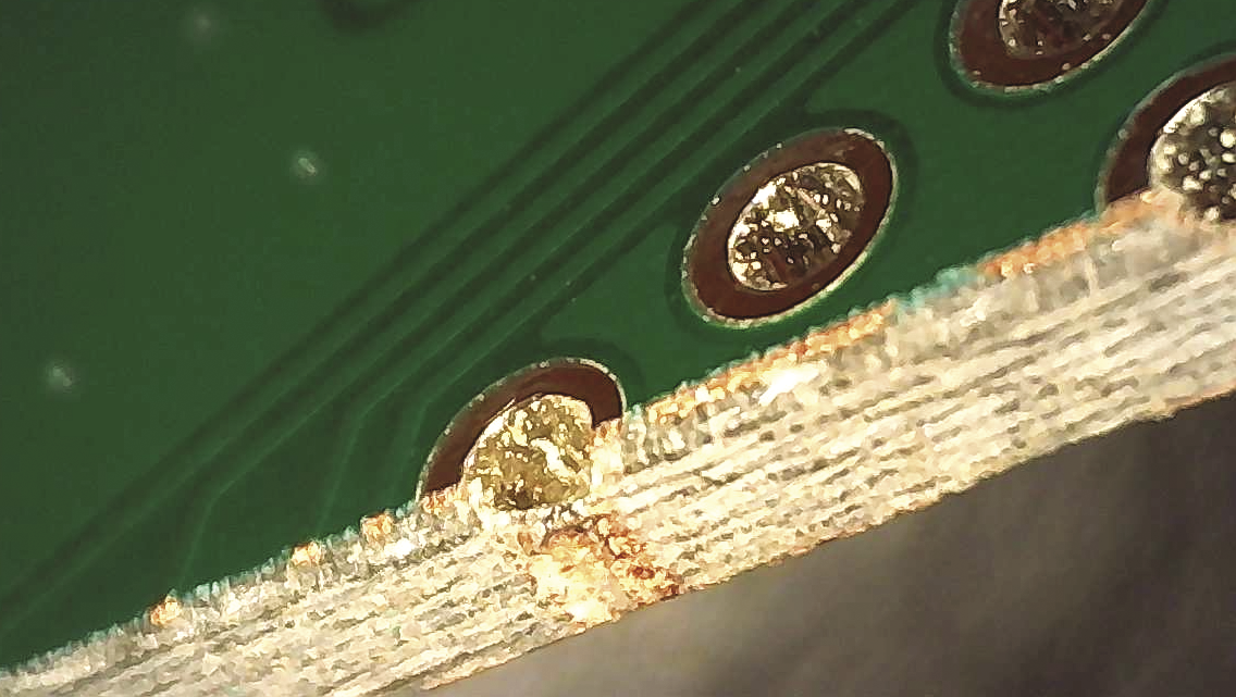
On top of the resist, an identification layer is printed by silkscreen printing that carries component identifiers (e.g., R1, C1, U1, J1), component outlines, polarization indicators (for diode and tantalum or electrolytic capacitors), and any other text or graphics you care to add. This layer is often colloquially know as the silkscreen layer, from the technique used to create it.
The process described so far has been highly automated, with PCB trace widths and spacings down to 0.1mm (4mil) being commonly available at very low cost and fast turnaround times. I’ll return to PCB production capabilities in the next article because it relates directly to the choice of design rules from the outset.
CAD Tools for PCB Design
Many PCB design tools are commercially available (e.g., Altium, OrCAD, and Allegro), some costing thousands of dollars per seat, and come equipped with tools to produce the most complex PCBs at the leading edge of technology. The open source tools are in my opinion no less impressive, and I’ve used one in particular over several years in a commercial setting, as well as for my own projects. I’ve yet to find a design for which KiCad cannot be used.
KiCad is a free and open source CAD tool originally developed at CERN. This excellent suite of tools handles the entire process of electronic design from schematic capture right through to generating files for manufacture. It is regularly updated with new, more powerful features and up-to-date component libraries (see the “What Is a Component?” box). Symbols and footprints not provided in the standard release can be downloaded from many websites.
A component is understood to be a resistor, capacitor, integrated circuit, and so on. In KiCad, they are described with symbols that describe a component for schematic capture and a footprint that describes the physical layout of pins and pads on a PCB layout to which the component will be soldered and PCB traces will be routed. KiCad provides libraries of the most common components, and manufacturers may also supply these symbols in many CAD formats, including KiCad. You can generate your own symbols or modify an existing one in the Symbol Editor. The KiCad libraries are read only, so if you modify a KiCad symbol, you must save your copy locally. If you edit a symbol already placed on a schematic, KiCad warns you that it is modifying the copy in the schematic only.
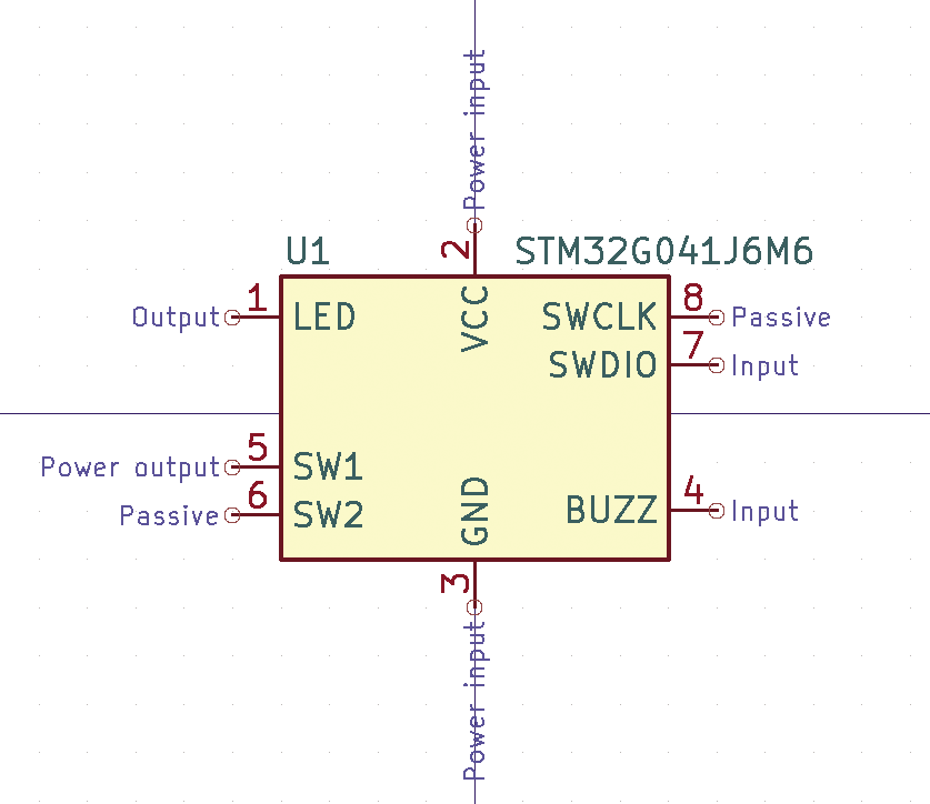
The simplest component is simply a rectangular box to which pins are attached (Figure 2). These pins represent the pins on the actual component and have names and numbers, which should closely match the information provided in the datasheet. The pin name is placed adjacent to the pin but outside the rectangle, and the pin’s functional name is inside the box. The symbol name (known as its Value) is usually chosen to match the manufacturer’s part number (e.g., STM32G041J6M6), although some symbols such as connectors have generic names (e.g., Conn_01x04, which denotes a four-pin connector arranged in one row). For resistors, capacitors, and inductors, the Value attribute is initially set to a default, and you can change it to reflect the value required by your design (e.g., 1.2K or 300p).
KiCad even has a 3D viewer that generates an image of your design, including the components, that can be panned and rotated. Although the PCB layout is in two dimensions, the ability to add 3D models of all the components and view the PCB assembly in a 3D viewer has saved me from mechanical clashes not apparent from the 2D design perspective. You can export the 3D model as a STEP file and import that into 3D CAD tools such as FreeCAD to build up more complex assemblies, aiding the design of such parts as enclosures that are suitable for 3D printing.
Workflow
Designing a PCB is a two-step process: schematic capture and PCB layout. In this article, I describe creating the schematic, and in the article to come, I’ll cover laying out the PCB. KiCad provides two separate tools for these processes: the Schematic Editor and the PCB Editor. The output of the Schematic Editor is called a netlist, although you rarely interact directly with it. The netlist data is a list of component footprints (a physical representation of a component’s pins) and a list of the connections between those pins.
The PCB Editor takes this netlist data as its input and, once the layout is complete, outputs manufacturing data in the form of a set of Gerber files, drill files, and other production data. The process of schematic capture for the netlist is essentially one of placing symbols that represent components on a schematic page and connecting the pins by drawing wires between them.
In any but the most trivial of designs this workflow is rarely linear: In the process of laying out the PCB, you will realize the schematic requires changes, or an idea for a new feature comes to you at a late stage. The PCB design can be updated with changes made to the schematic: adding or removing components, changing component attributes such as its footprint (more on footprints later), adding wires, and even changing the size and shape of the final PCB. Sometimes, you’ll want to switch interchangeable pins (e.g., the inputs to an AND gate) to help with track layout.
Installing KiCad
If you head over to the KiCad homepage and click Download, you’ll be presented with a choice of target operating systems. Choose one (Linux, obviously!) and follow the instructions to install the stable release for your distro. The install includes not only the KiCad tools themselves, but the symbol and footprint libraries you’ll use in your design.
KiCad Project Interface
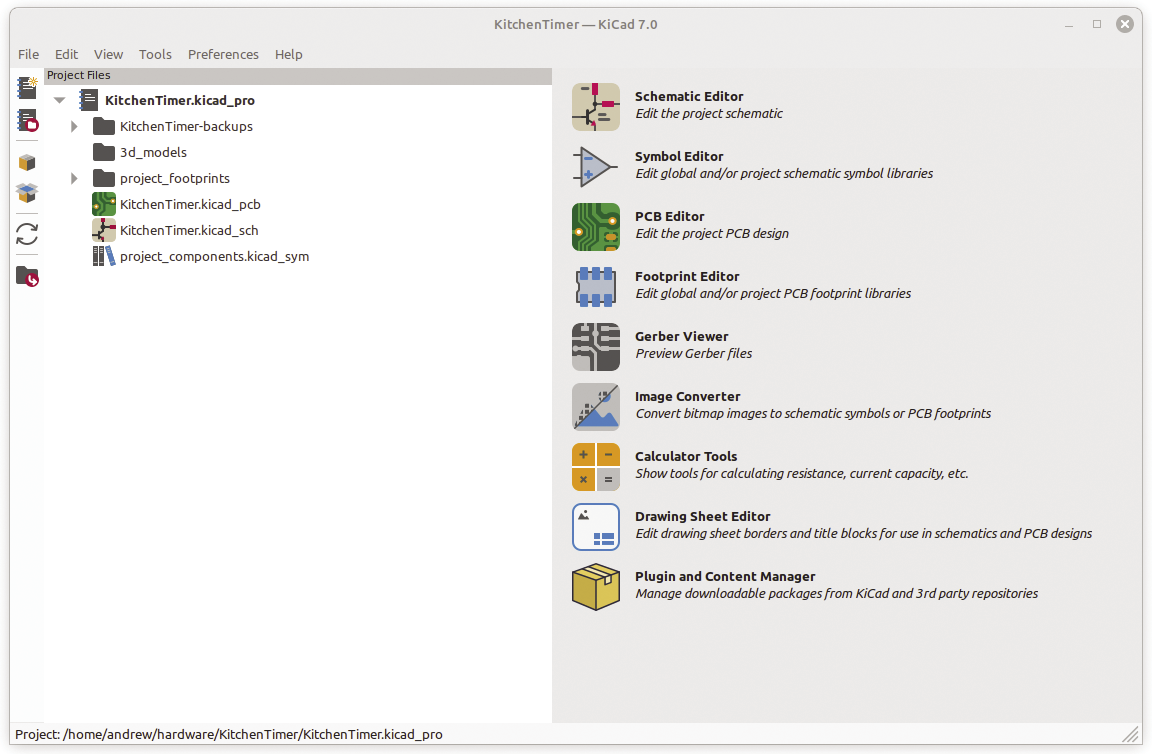
When you launch KiCad (Figure 3), the left side of the main window shows a directory listing of the various files that make up your project, and the right side has the available tools, which you can launch individually. On my distro, they are all available from the launch menu, which is useful if, for instance, you want to cut and paste parts of an existing schematic into the current project. However, in the normal workflow, as will become clearer later, you need to launch the Schematic Editor from the project interface to be able to go back and forth between the PCB design and schematic in the project.
Creating the Schematic
After clicking the Schematic Editor icon in the project interface, you’ll see a new window with a drawing sheet. The File menu has submenus that allow you to customize the appearance of the drawing or replace the drawing sheet with a different template. (The project interface has a template editor icon that allows you to create your own template.) For now, the default template is sufficient. The symbols you add to the schematic are in real-word units; that is to say, they do not scale with the paper size, so a larger page gives you more room to add symbols to your design.
If you plan to print your schematic, you can select the paper size from Page Settings. For larger projects, I prefer to select an A3 paper size with more drawing area for my design, which can still be printed to A4 at a later date. My US friends have US letter options. For the example here, I used the smallest (A5) sheet size, which is more than sufficient for the example schematic.
To start adding symbols to the drawing, select the Place | Add Symbol menu item. Select OK and the symbol will be dropped onto the drawing sheet. Move it to the center of the sheet and click the mouse to place it. You can move it around later. If you click the mouse again, you will be presented with the Choose Symbol dialog again so you can select and add the next symbol. Alternatively, press Escape to exit the add symbol mode.
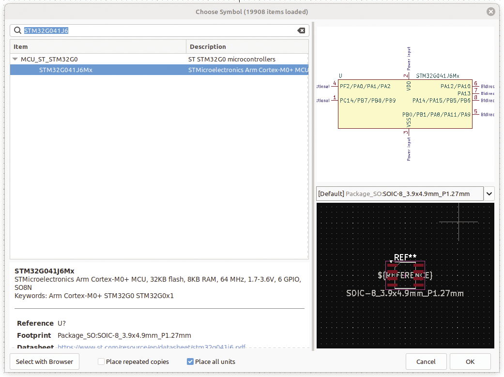
To add resistors and capacitors, simply type r or c in the Choose Symbol dialog (Figure 4). These are generic symbols and have no default footprint or value: I will come back to assigning these later. For polarized capacitors such as electrolytics and tantalums, you can use the symbol C_Polarized. KiCad provides a vast selection of symbols, and you can search for the one you want by name or scroll through the list below the search box. If you can’t find what you need, you can either select the nearest match and edit the local copy or create your own from scratch (more on that later).
If you want to follow along with the working example (see the “A Kitchen Timer Example” box), you can search for and add the following symbols:
- SW_Push x 2
- LED_Filled
- R (resistor)
- C (capacitor)
- C_Polarized (polarized capacitor)
- Buzzer
- Jumper_2_Bridged
- Conn_01x05 (generic 5 pin connector)
- Battery
- Mounting_Hole x 2
Don’t worry about placement for the moment; just drop them on the sheet and go back for the next one. You can even drop them outside the schematic border until you are ready to move them into position.
A similar action is used to add power nodes with Place | Add Power; you can search for and add the following:
- +3V
- GND
These nodes allow you connect all the power and ground pins together without wires between them. They are not strictly necessary, but they make the schematic much easier to read because they eliminate at least two wires that visit all the power nodes. If the nodes have the same name, they will be electrically connected. To exit from Place mode, press the Escape key.
Now you can begin arranging the components on the schematic. To move a component, simply click and drag. In a later section of this article, I show you how to lay the symbols out roughly to make the subsequent wiring easy to read without too many crossovers and long, serpentine wires. You will need to duplicate the power and ground nodes by selecting them with the mouse and pressing D. You can move the duplicated node to the desired position. The same technique works for components, which can be a great help when building schematics with lots of similar components, such as resistors. In this case, the component reference (e.g., R1) is incremented automatically, so you don’t end up with two R1s.
Note that once the symbols are placed, you can start to add the connections (wires) between them. If you click on the small circle at the end of a pin on a symbol, wire drawing mode starts. Drag the mouse to draw the wire and left-click to add a corner. Wire drawing stops when you click on another pin or if you right-click and select Finish wire or Cancel. If you want to move an already connected component, select it and press G. As you move the component, the wire will rubber-band to stay connected. Be careful, though, because it is easy to connect two wires together inadvertently if they overlap when you have finished moving the component.
The usual Ctrl+Z undo is available if you make a mistake, and cut, copy, and paste operations all work with the standard key combinations on selected items: Just select a block of the schematic by clicking on an unused area and drag over the symbols and wires you want to select before using the appropriate keystrokes on the block. This process works within a sheet, from sheet to sheet, and even from project to project, which is very useful as you build up a number of designs: You can use them as a library to pull in functional blocks (e.g., power supplies, custom symbols, or filters) to speed up entering a new design. Reusing parts of designs like this can also help eliminate errors, assuming the original has been built and tested and you keep the schematic up to date with any corrections you make. The metadata associated with the copied symbols, such as footprint references, are copied too.
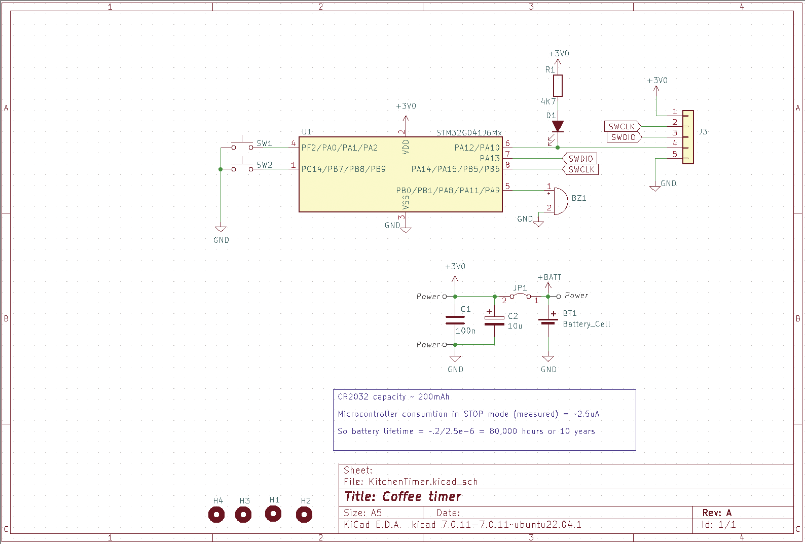
Returning to the example, the only incomplete connections are those that end in flags marked SWCLK and SWDIO: These are signals from the off-board programmer to the microcontroller. Although they could be connected directly with wires, for clarity I’ve used global labels, which you add with Place | Add Global Label. In the dialog that opens, you type the name of the signal or wire and drop the label on the schematic. The label has a virtual pin to which you can connect a wire; labels with the same name will be connected together, just like the power symbols.
These labels are the only way to connect symbols on different pages or sheets in the same design but are also very useful within a single sheet because they reduce visual clutter. Although I don’t cover multiple pages in this example, it becomes necessary with larger designs and allows the design to be organized by function (e.g., I/O on one page, power supply on another, microcontroller and peripherals on a third, and analog circuitry on a fourth). Much as a software engineer organizes parts of a program into files, this technique helps you visualize the overall structure and find more quickly the parts of the design you want to use.
Component Values
Once you have the components in place and wired up, you can add values to components such as resistors and capacitors. For example, a resistor will have the default value R alongside its identifier (e.g., R2). To enter a value, double-click on the R. Of course, this value is for documentation only and is not strictly necessary to produce a PCB, but the schematic is also used for debugging, and you can generate parts lists from the values you enter.
Components such as integrated circuits have their values set to their part number (e.g., STM32G041J6Mx), so often you do not need to change them. A word of caution, though: Some integrated circuits exist in different forms and even have different pinouts, so make sure you’ve selected the correct one. This is typically achieved with part numbers that have suffixes that denote the physical package – e.g., an SN74LS00NSR is a quadruple NAND gate in a through-hole plastic dual in-line package (DIP), whereas an SN74LS00D has the exact same function in a small outline integrated circuit (SOIC) surface-mount package.
If two versions exist with different pinouts – e.g., ball grid array (BGA) and plastic-leaded chip carrier (PLCC) – they should have corresponding symbols in the KiCad library. You can amend the assigned part number to reflect the package you want (and assign the correct footprint – see below), so that any parts list you generate will lead to buying the correct part variant. I have encountered this pitfall many times.
Connectors and similar parts will have values, too: In the case of the five-pin connectors in the example, the value will be Conn_01x05, which isn’t really helpful, so you can either hide it (double-click and untick Visible) or change it to reflect the connector’s function (e.g., Debug Port). I prefer to hide the value and annotate the connector’s function with text (Place | Add Text), because the text is a different color and stands out.
Finally, if you click on a value or identifier, you can move it around by pressing M and rotate it by pressing R to help tidy the schematic and make it clear to which component these values belong.
Component Numbering and Annotation
If you’ve copied parts from another KiCad schematic or deleted components during schematic entry, you might notice that the identifiers (R1, R2, etc.) are not sequential. Before moving onto the PCB layout, you can annotate the schematic from Tools | Annotate and select the Reset Existing Annotations option to ensure sequential identifiers. You can even do this once layout has started; KiCad keeps a unique internal identifier for each component, and the visible identifier is just another attribute attached to that identifier.
Non-Electrical Parts
Some parts you might want to add to your schematic will be non-electrical, such as mounting holes that are not plated. Putting them on the schematic allows you to assign a footprint, which in turn determines the hole size required and places a “courtyard” around the hole to prevent the placement of a component too close that might interfere with any fastener placed through the hole. Other non-electrical items might be a fuse. A fuse holder will have connections, but if you want the fuse to appear in your parts list, you can add a fuse that has no pins. Other components in this category are decals and trademarks that appear only on the silkscreen.
Preparing for Layout
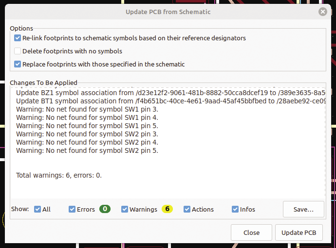
Before you can begin to lay out the PCB, you must ensure that all the data about the chosen components the layout requires is available. If you attempt to begin layout without this data, the transfer to the PCB layout will be, at best, partial and can be very confusing. Transfer to the PCB is achieved by Tools | Update PCB from Schematic, which opens the PCB tool and loads any layout in the same folder with the same name as the schematic or creates an empty layout (Figure 5). If the update dialog indicates errors, it’s best to press Close and go back to fix them. No changes are made unless you select Update PCB.
Footprints
If you’ve used only standard symbols from the KiCad libraries, there’s a good chance they all have an assigned footprint. You can check by selecting a symbol and pressing F. A dialog to select the footprint appears (Figure 6). If the footprint entry is not blank, the component already has a footprint assigned. Click on the icon to the right of that field, to check the footprint.
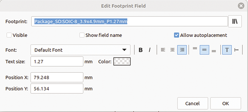
The footprint library editor opens, and you can make sure the selected footprint matches the datasheet of the component you have selected. Pay close attention! Many components come in packages with several variants, some of which look very similar but have different pin or pad spacing. There’s nothing more frustrating than receiving a PCB only to discover the components don’t fit. Check and double-check! To avoid visiting every component in the schematic individually, you can get an overview from the Tools | Edit Symbol Fields dialog (Figure 7).
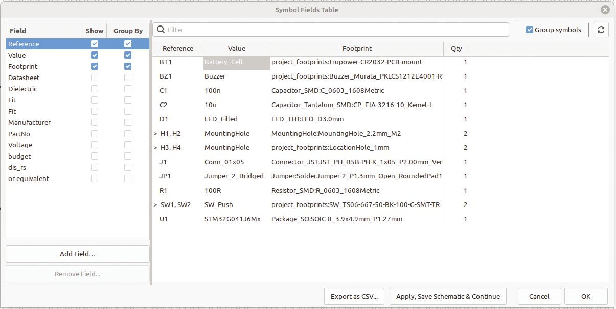
The third column of this table shows the footprint for each component and is editable in the same way as in the previous dialog. From here you can ensure every component has a footprint and that it is correct. Whilst you are here, you can also check that all components have sensible values. You can add custom columns, such as in-house part numbers, cost estimates, and links to datasheets.
Net Class Directives
The connections between component pins, collectively known at “nets” may be grouped into classes so that they can be treated differently in the layout tool. By default, nets fall into a general class and most will remain there. Power nets, such as +3V and GND benefit from wider tracks in the layout, and sensitive analog tracks might also require special treatment. KiCad allows you to add an attribute to nets with Place | Add Net Calls Directive. In the case of the example, the two power nets +3V and GND are labeled with a directive called Power. The name itself is unimportant, so chose something meaningful in this context. When you are ready to set up the board for layout, you’ll see how to use these directives to give different physical characteristics for these nets.
Net Labels (USB Example)
All nets are given unique names by KiCad, and for the most part, you do not need to override them. You can do so, however, with the Place | Add Label item. Nets that are connected with the global labels described above are similarly renamed. If your design has differential pairs that you want to route together, you need to name those nets according to the differential routing tool in the layout; for example, nets labelled USB+ and USB- will be eligible for routing as a differential pair.
Parts Lists
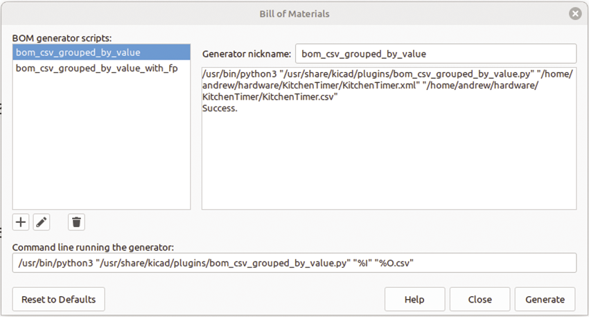
Parts lists are generated with Tools | Generate BOM (Figure 8). BOM stands for “bill of materials” and is a common term interchangeable with “parts list.” This tool generates an XML file that you can process further and optionally runs a script that extracts the data from the schematic through a Python interface. I use a modified form of this project to produce a BOM in my required format. A number of third-party plugins are available for KiCad, and I would encourage you to do some searching to find those that suit your particular needs.
If you double-click on a symbol to show the properties, you’ll see an option to exclude a symbol from the BOM, which is useful for symbols such as mounting holes, which are just artifacts of the PCB and obviously can’t be purchased. Likewise, you can exclude a symbol from the board layout for things such as fuses, as mentioned previously, that need to be on a parts list and on the overall PCB assembly but are not fitted directly to the PCB.
Other Documentation
Other Place menu items are useful for adding documentation to your schematics. In this example (see the “Kitchen Timer Example” box), I’ve added a text box with a brief estimate of battery lifetime. You can place images and draw lines and circles, as well. The Place | Rectangle option can be useful if you want to delimit some part of your schematic in some way, perhaps to document a sensitive analog area that should be kept separate or a high voltage area that requires additional spacing. The rectangle has properties: You can make it dotted, fill the interior with a color, and so on. Be aware that none of these documentation features affect your PCB layout in any way; they are simply a way to record information on the schematic that you can refer to during the layout process. If layout is to be performed by another person, this documentation is an excellent was to ensure they have all the information needed to complete a successful layout.
The example I work though in the next article is a simple kitchen timer (Figure 9) with the following characteristics:
• Two timer buttons: coffee – 5 mins and pizza – 25 mins
• CR2032 battery cell with a lifetime greater than one year
• A 32-bit ARM microcontroller in an eight-pin SOIC package
• A piezoelectric buzzer to indicate the end of period
• An LED/serial output for debugging
• Small, wipeable enclosure 35x35x15mm (1-3/8 x 1-3/8 x 5/8 inches)
The firmware for the project is available on my GitHub page.
Electrical Rules Checker
In my next article, I check the layout for design rule violations, which is an important part of ensuring your design can be manufactured and will function as intended. The schematic tool has a similar design rule checker available under Inspect | Electrical Rules Checker. The errors flagged by this tool are often cosmetic and can be ignored, but it is useful to run it nonetheless. For example, it warns of unconnected pins, which may be deliberate, but it is worth checking that your drawn wires actually attach to pins and don’t stop short. Other errors are along the lines of Error: Input Power pin not driven by any Output Power pins.
If you use the symbol editor to look at a component symbol, you will notice individual pins are labeled Input, Output, or Passive. KiCad would like to see an input driver by an output, but many symbols in the component library (and most that you can import from manufacturer websites) set all the pins to Passive, and that gives rise to these “errors.” You can simply ignore them or edit the local symbols in your design to ensure one pin on each wire is an output. When you are happy with your schematic, you can click Delete All Markers to remove the markers that are placed on the schematic.
Pins themselves have attributes (e.g., Input, Output, Passive) for documentation or for use in circuit simulation, so they can be ignored for now. More importantly, KiCad symbols themselves have a number of linked attributes, the most important being the Footprint, which is the layout of pads and holes in the physical PCB. I cover footprints in more detail in the second article. For now, it’s enough to know that each symbol you place on the schematic must have a footprint assigned before you can generate the initial PCB file. You can add your own attributes to document your design, such as working voltage, tolerance, supplier part number, and so on.
Wrap-Up
So far, you learned to capture your electronic design ideas in schematic form, prepare the schematic in anticipation of PCB layout, and produce a parts list from which you can order parts to build a prototype – or give to a manufacturer to assemble the prototypes for you. You can also estimate the BOM cost at this point, which will allow you to budget for purchase or, in a commercial setting, allow others in your team to assess the commercial viability of the design. You’ve performed some basic checks to ensure the schematic is correct, and you may have transferred the analog parts of your circuit to a simulator such as PSpice to ensure it functions as intended. Finally, you’ve performed some basic electrical checks and added some documentation.
In the final article in this series, I discuss transferring the design to the layout tool, placing the parts, and wiring them up. With this process complete, you’ll be ready to send files to your manufacturer and start building your prototypes.

